Cerebras Unveils CS-4 Roadmap Targeting 30x Faster AI Than GPUs
Cerebras unveiled the CS-4 wafer-scale system architecture at Hot Chips and sketched a roadmap to CS-5 and 3D-stacked DRAM in CS-6.
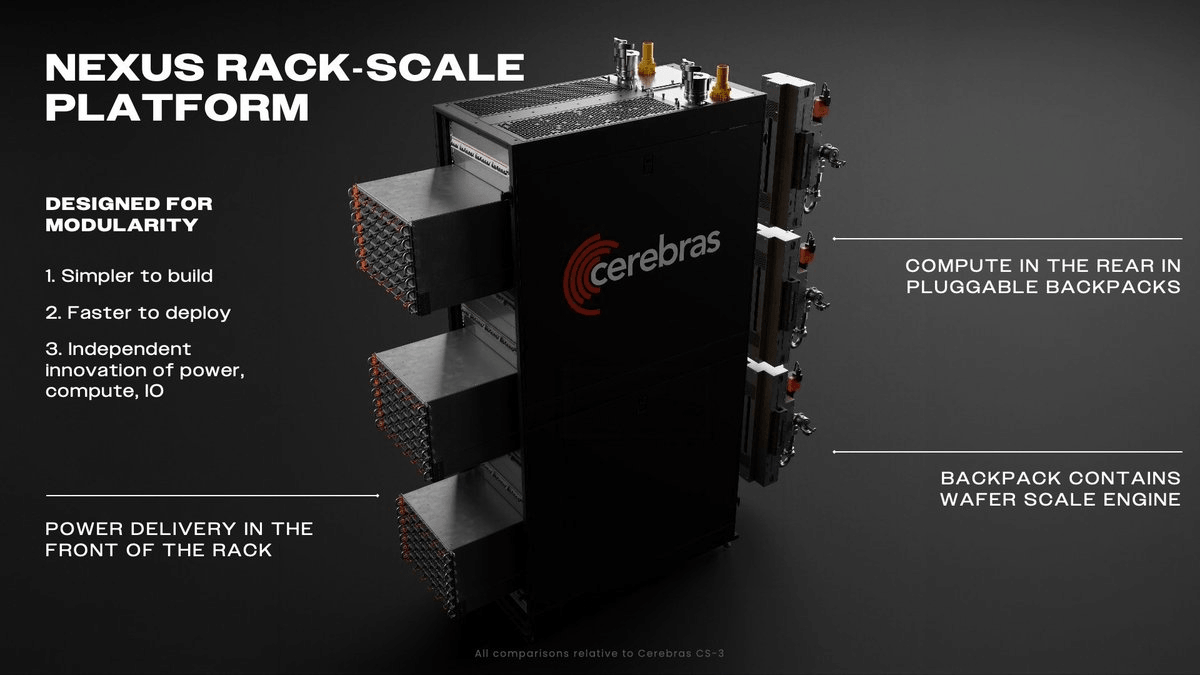
- Cerebras detailed CS-4 architecture at Hot Chips 2026, with GA scheduled for Q3 2026.
- CS-4 packs three WSE-3 Turbo wafers per Nexus rack, delivering 750 PFLOPs and 2x faster tokens vs CS-3.
- Power converters sit 0.5mm from the wafer, 100x closer than GPU boards, enabling double the clock speed.
- A single WSE-3T offers 53.5 PB/s of on-wafer bandwidth, roughly 200x an NVIDIA NVL72 rack's NVLink.
- CS-5 (2027) targets 10,000 tokens/sec/user on gpt-oss-120b and 5,000 tokens/sec/user on trillion-parameter models.
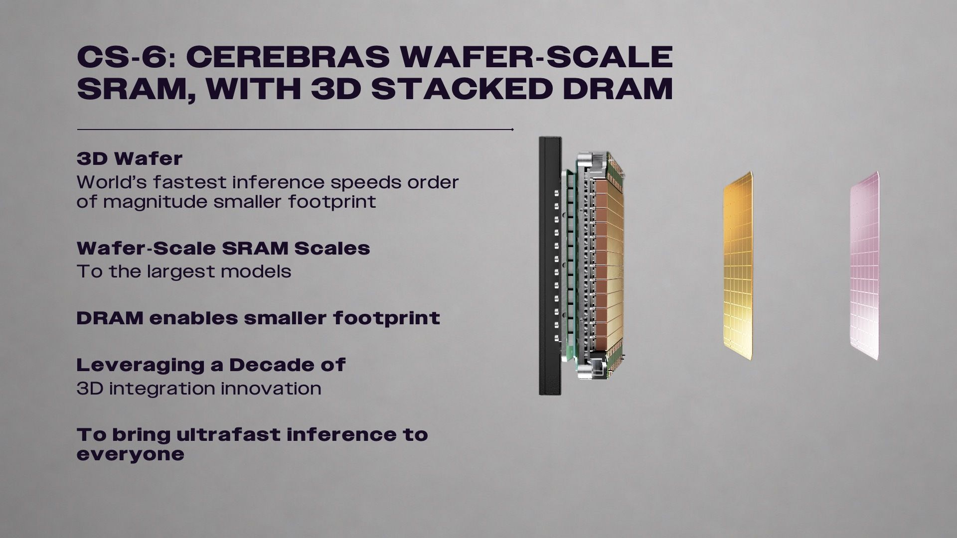
- CS-6 integrates 3D-stacked DRAM on wafer-scale SRAM, expanding memory without breaking data locality.
Cerebras used its Hot Chips 2026 slot to open up the internals of the CS-4, its newest wafer-scale AI accelerator, and to lay out a two-generation roadmap that leans harder into a bet the rest of the industry keeps trying to work around: keep the compute on one giant piece of silicon, and iterate on the rack around it. The deep dive covers CS-4's power, cooling, and I/O design, previews CS-5 for 2027, and introduces CS-6, which stacks DRAM in 3D on top of a wafer-scale processor.
The rack is now the product
CS-4 is the first system built on Nexus, a reusable rack-scale platform. Three WSE-3 Turbo wafers sit in a redesigned Nexus rack with doubled per-wafer power delivery, direct liquid cooling, and a new Ethernet-based scaling fabric. Each wafer lives in a modular compute backpack at the rear of the rack, with its own power conversion, cooling loop, and I/O. The front rack goes into the datacenter first, and the backpacks drop in on-site, compressing deployment from days to hours.
Cerebras claims CS-4 delivers up to 2x faster tokens per second than CS-3, and up to 30x faster performance than GPU solutions on frontier models. Per-wafer, CS-3 hit 125 PFLOPs on a single WSE-3, while CS-4 offers 750 PFLOPs across three WSE-3T chips at 250 PFLOPs each. The rack is in early access with general availability scheduled for Q3 2026.
Power delivery gets a millimeter, not a meter
The most striking architectural detail is where the power converters live. In a conventional GPU board, current has to travel roughly 50 millimeters across a PCB through stacked copper layers before it reaches the silicon, wasting energy as heat and constraining how much current you can push at a given voltage.
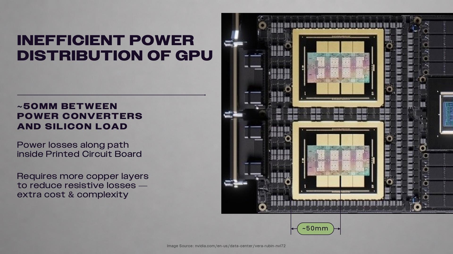
Cerebras moved its AC/DC converters to about 0.5 millimeters from the wafer, with no PCB in the final power path. The result is roughly twice the power at nearly the same voltage, with very little resistive loss. That is what makes the WSE-3 Turbo variant work at all: converters positioned half a millimeter from the processor enable double the clock speed without redesigning the underlying 5nm silicon.
Cooling and rack integration
Each backpack ships with its own water-conditioning module, an energy meter that tracks flow and inlet/outlet temperature, and an actuator that modulates flow to the cold plates. Dry quick-disconnect valves let technicians pop a backpack out without draining the loop, and leak sensors can trip the module into a safe state and cut power. Water and compute stay at the back of the rack, high-voltage AC lives at the front, and manifolds run down the sides so a single backpack can be swapped without touching shared infrastructure.
Front-of-rack power supports several redundancy configurations, and the AC feeds are phase-balanced across up to six hard-wired inputs. It reads like a design driven by hyperscaler operations teams as much as by the chip architects.
Why wafer scale keeps compounding
The core argument for wafer scale has always been on-chip bandwidth. Cerebras put a specific number on it this time: a single WSE-3T provides 53.5 petabytes per second of aggregate on-wafer fabric bandwidth. For comparison, NVIDIA specifies 260 terabytes per second of rack-level NVLink bandwidth for an entire 72-GPU Rubin rack, whose NVLink spine uses roughly 5,000 internal cables. That is a 200x gap in scale-up bandwidth between one wafer and one NVL72.
The practical consequence shows up at small batch sizes and in mixture-of-experts routing, where communication overhead can be as expensive as the actual matmul. When a model spans multiple Cerebras systems, execution is pipelined so that high-volume tensor and expert traffic stays inside a wafer, and only activations cross between them. That looks very different from lashing thousands of accelerators together with an optical spine.
CS-5 aims at 10,000 tokens per second per user
CS-5, targeted for 2027, is where Cerebras plans to push token-generation speed into territory that current GPU systems cannot approach. The company is targeting up to 10,000 output tokens per second per user on leading open-source models like Gemma 4 31B and gpt-oss-120b. For multi-trillion-parameter frontier models such as Kimi and GPT-5.6 Sol, it targets up to 5,000 tokens per second per user and 3 million tokens per second per megawatt, with the same architecture designed to handle models over 50 trillion parameters at interactive speeds.
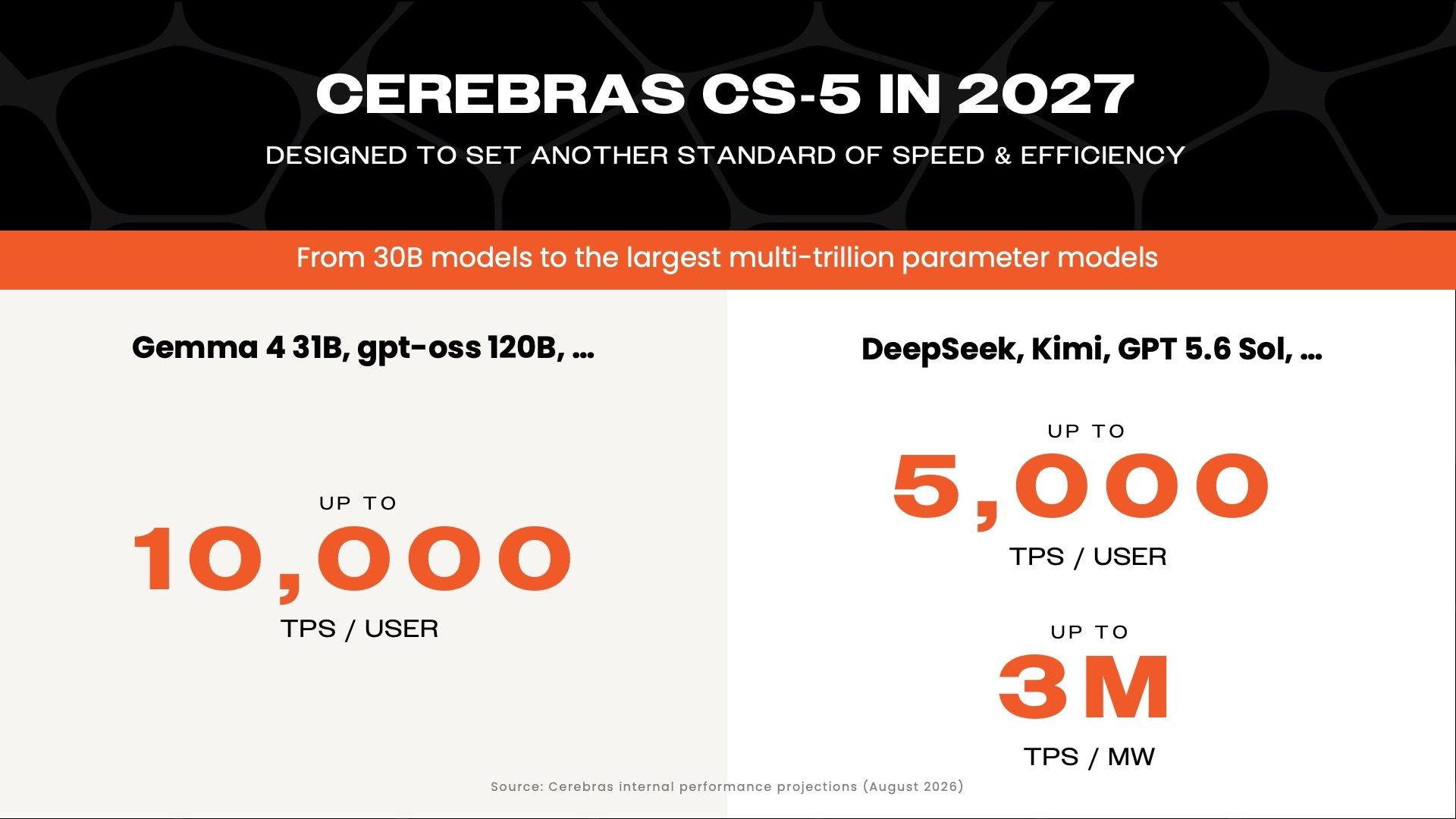
Those numbers matter for agents, not chatbot latency. Agentic workloads chain many sequential model calls, so per-user output speed multiplies into total task-completion time. If each step is 10x faster, a 20-step agent chain feels 10x more responsive end to end.
CS-6 goes vertical
A wafer already occupies the largest practical 2D area silicon manufacturing allows. The only remaining direction is up, and CS-6 is where Cerebras takes it. The system integrates wafer-scale SRAM and compute with 3D-stacked DRAM through ultra-high-bandwidth vertical connections, expanding memory capacity without breaking the data locality that makes wafer scale fast in the first place.
The pitch:
- More of each model resides on each system, cutting the number of wafers needed to serve trillion-plus-parameter models
- Smaller physical footprint per deployed model, in some cases an order of magnitude smaller
- Preserved on-wafer bandwidth advantage, since DRAM sits directly above compute rather than across a rack
What to take away
Cerebras is treating the rack, rather than the chip, as the unit of iteration. Nexus is designed so that power, cooling, I/O, and the wafer itself can be upgraded independently, which is how the company can promise roughly a doubling of token-generation speed per year without waiting on a full silicon respin. CS-6's 3D memory stacking then targets the weakness that has historically kept wafer-scale from serving the largest models: on-die SRAM capacity. If it lands, the argument that GPUs are the only economical way to serve trillion-parameter models loses some of its force.
For anyone building latency-sensitive inference, especially agents that chain many model calls, this roadmap is the clearest signal yet that per-user token speed is becoming a first-class dimension of hardware competition alongside throughput per dollar.
Comments